- 您现在的位置:买卖IC网 > Sheet目录362800 > EVAL-AD421EB (Analog Devices, Inc.) Loop-Powered 4 mA to 20 mA DAC
AD421
–
12
–
REV. C
DV
DD
AV
DD
REF IN
CS
DATA OUT
SCLK
DATA IN
AGND
DGND
MCLK IN
MCLK OUT
AD7714/
AD7715
ANALOG
TO
DIGITAL
CONVERTER
SENSORS
RTD
mV TC
REF OUT1
BOOST
V
CC
LV
COMP
DRIVE
LOOP
RTN
REF OUT2
REF IN
CLOCK
LATCH
DATA
COM
C1
C2
C3
LOOP
POWER
0.01 F
DN25D
2.2 F
3.3V
1.25V
4.7 F
AMBIENT
TEMP
SENSOR
AD421
MICROCONTROLLER
V
CC
GND
WAVEFORM
SHAPER
BANDPASS
FILTER
HART
MODEM
BELL 202
0.1 F
0.01 F
1k
1000pF
C
C
*
HT20C12/20C15
4.7 F
100k
*FOR SELECTION OF C
C
, REFER TO AN-534
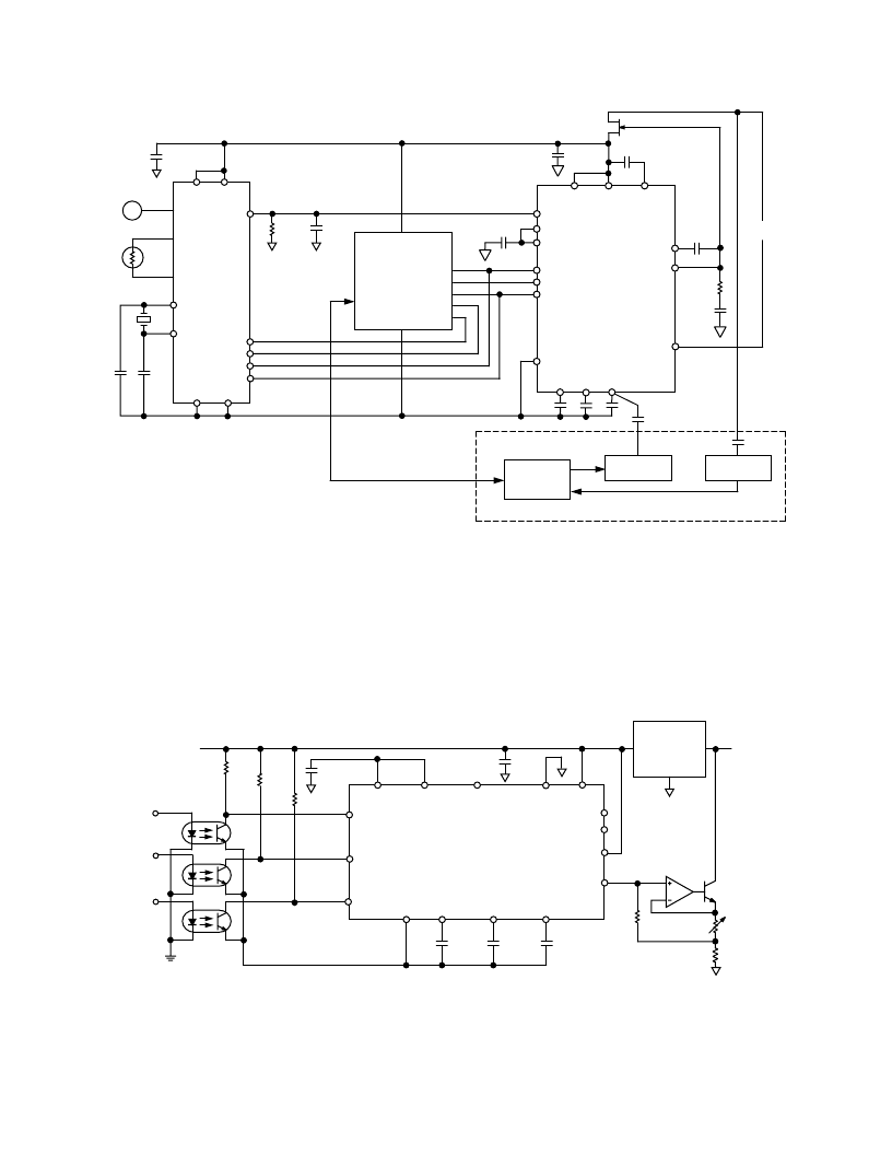
Figure 17. AD421 in HART Transmitter Application
across R2. The ratio of R1 to R2 determines the current that
flows in the load resistor R
L
.
I
L
= [1 +
R
1
/R
2]
×
I
PROG
, where I
L
is the current that flows in the load resistor R
L
and I
PROG
is the
current programmed to the AD421. R1 and R2 are external to
the AD421 and will need to be matched resistors to obtain a
highly accurate current source.
Current Source
Figure 18 shows an application circuit for the AD421 being
used as a current source. The current programmed to the
AD421 (4 mA to 20 mA) will develop a voltage across R1.
This same voltage due to negative feedback will be generated
LOOP
RTN
R2
R
L
R1
C1
C2
C3
COM
V
CC
LV
2.2 F
COM
DRIVE
COMP
BOOST
0.01 F
0.01 F
0.0033 F
LATCH
CLOCK
DATA
REF IN
REF OUT2
REF OUT1
4.7 F
COM
AD421
+5V
10k
10k
10k
CLOCK
LATCH
DATA
V
S
RETURN
5 VOLT
REGULATOR
OUT
IN
V
S
COM
Figure 18. AD421 in Programmable Current Source/Sink
发布紧急采购,3分钟左右您将得到回复。
相关PDF资料
Eval-AD5025EBZ
Fully Accurate 12-/14-/16-Bit VOUT DAC SPI Interface 2.7 V to 5.5 V in a TSSOP
Eval-AD5045EBZ
Fully Accurate 12-/14-/16-Bit VOUT DAC SPI Interface 2.7 V to 5.5 V in a TSSOP
Eval-AD5065EBZ
Fully Accurate 12-/14-/16-Bit VOUT DAC SPI Interface 2.7 V to 5.5 V in a TSSOP
EVAL-AD5066EBZ
Fully Accurate 16-Bit UnBuffered VOUT DAC SPI Interface 2.7 V to 5.5 V in a TSSOP
EVAL-AD5379EB
40-Channel, 14-Bit, Parallel and Serial Input, Bipolar Voltage-Output DAC
EVAL-AD5381EB
40-Channel, 3 V/5 V, Single-Supply, 12-Bit, Voltage Output DAC
EVAL-AD5382EB
32-Channel, 3 V/5 V, Single-Supply, 14-Bit, Voltage Output DAC
EVAL-AD5383EB
32-Channel, 3 V/5 V, Single-Supply, 12-Bit, Voltage Output DAC
相关代理商/技术参数
EVAL-AD5025EBZ
制造商:AD 制造商全称:Analog Devices 功能描述:Fully Accurate 12-/14-/16-Bit VOUT DAC SPI Interface 2.7 V to 5.5 V in a TSSOP
EVAL-AD5045EBZ
制造商:AD 制造商全称:Analog Devices 功能描述:Fully Accurate 12-/14-/16-Bit VOUT DAC SPI Interface 2.7 V to 5.5 V in a TSSOP
EVAL-AD5060EB
制造商:Analog Devices 功能描述:EVAL BD FOR AD506X DAC 14-/16BIT, SERL INPUT - Bulk
EVAL-AD5060EBZ
功能描述:BOARD EVAL FOR AD5060 RoHS:是 类别:编程器,开发系统 >> 评估板 - 数模转换器 (DAC) 系列:nanoDAC™ 产品培训模块:Lead (SnPb) Finish for COTS
Obsolescence Mitigation Program 标准包装:1 系列:- DAC 的数量:4 位数:12 采样率(每秒):- 数据接口:串行,SPI? 设置时间:3µs DAC 型:电流/电压 工作温度:-40°C ~ 85°C 已供物品:板 已用 IC / 零件:MAX5581
EVAL-AD5061EBZ
功能描述:BOARD EVALUATION AD5061 RoHS:是 类别:编程器,开发系统 >> 评估板 - 数模转换器 (DAC) 系列:nanoDAC™ 产品培训模块:Lead (SnPb) Finish for COTS
Obsolescence Mitigation Program 标准包装:1 系列:- DAC 的数量:4 位数:12 采样率(每秒):- 数据接口:串行,SPI? 设置时间:3µs DAC 型:电流/电压 工作温度:-40°C ~ 85°C 已供物品:板 已用 IC / 零件:MAX5581
EVAL-AD5062EB
制造商:Analog Devices 功能描述:EVAL BD FOR AD506X DAC 14-/16BIT, SERL INPUT - Bulk
EVAL-AD5062EBZ
功能描述:BOARD EVAL FOR AD5062 RoHS:是 类别:编程器,开发系统 >> 评估板 - 数模转换器 (DAC) 系列:nanoDAC™ 产品培训模块:Lead (SnPb) Finish for COTS
Obsolescence Mitigation Program 标准包装:1 系列:- DAC 的数量:4 位数:12 采样率(每秒):- 数据接口:串行,SPI? 设置时间:3µs DAC 型:电流/电压 工作温度:-40°C ~ 85°C 已供物品:板 已用 IC / 零件:MAX5581
EVAL-AD5063EB
制造商:Analog Devices 功能描述:Evaluation Board For 14-/16-Bit, Serial Input, Vout NanoDACs 制造商:Analog Devices 功能描述:EVAL BD FOR AD506X DAC 14-/16BIT, SERL INPUT - Bulk